

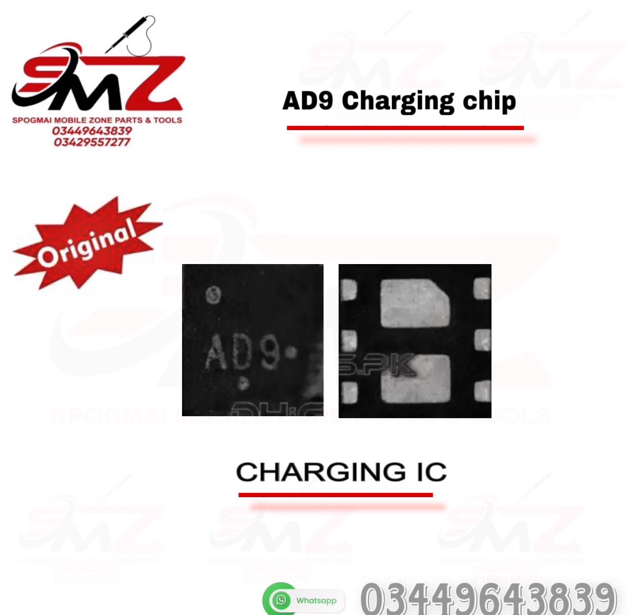
Key Technical Overview
- Primary Function: It drops the standard 5V USB input down to a safe battery-charging threshold (typically between 3.7V and 4.2V).
- Common Applications: Keypad mobile boards, small Bluetooth speakers, and clone devices.
- Failure Symptoms: If the AD9 IC burns out or degrades, the device will exhibit “fake charging” (showing the charging icon but not increasing battery percentage), a completely dead power state, or extreme overheating near the charging port.
Common Substitutes and Solutions
If you cannot source an exact AD9 replacement chip during a mobile repair, technicians commonly use alternative methods:
- The “Easy Charge” Universal Module: You can bypass the broken onboard IC entirely by soldering a miniature 3-pin or 5-pin Universal Power Charging Board into the phone’s casing. [1, 2, 3]
- Zener Diode Jumper Method: A classic hardware workaround involves removing the broken AD9 chip and soldering a 5V or 4.7V Zener diode between the positive USB input pin (\(V_{\text{BUS}}\)) and the positive battery connector terminal (\(V_{\text{BAT}}\)). This forces a direct, simple charge flow into the battery.




Reviews
There are no reviews yet.