

Key Technical Specifications
- Charging Capability: Delivers up to a 6-A fast-charging current in a parallel, dual-charger configuration.
- Input Voltage Range: Supports 3.9 V to 14 V operational input (with a 20-V absolute maximum rating) to accommodate high-voltage fast chargers.
- Input Current Limit: Programmable from 500 mA to 3.6 A to comply with USB 2.0, USB 3.0, and standard adapter safety requirements.
- Efficiency: Highly efficient 750-kHz operating frequency, achieving up to 95.4% efficiency at 1.5 A (5-V input).
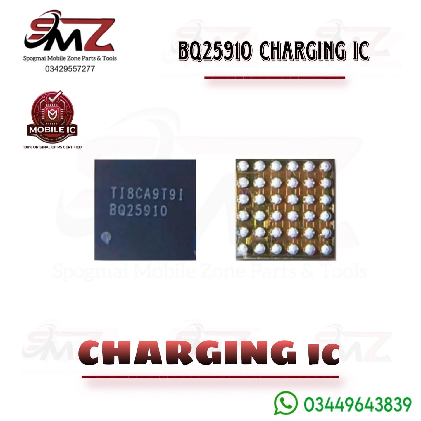
- Package Type: Manufactured in a compact 36-ball Wafer Chip Scale Package (WCSP).
Main Functions & Features
- Three-Level Buck Architecture: Dramatically reduces solution footprint and inductor ripple, letting manufacturers use low-profile inductors while maximizing power density.
- High Integration: Houses all internal power MOSFETs, lossless current sensing (no external sense resistor needed), and loop compensation.
- Safety Protocols: Features thermal shutdown, battery overvoltage protection (OVP), input overvoltage protection, flying capacitor short-circuit prevention, and input Dynamic Power Management (VINDPM).
Common Use & Repair Applications
Because this IC regulates the primary power delivery path, it is frequently replaced by technicians during board-level smartphone repairs. Common symptoms indicating a faulty BQ25910 IC include a device refusing to charge altogether, failing to register fast charging, overheating near the power section, or causing a total motherboard short-circuit due to a faulty charger or water damage. Replacement chips can be easily sourced for repair from platforms LIKE SMZ.
Reviews
There are no reviews yet.