

🛠️ Key Technical Specifications
The official SGM41512 Datasheet outlines the following core electrical characteristics:
-
- Input Voltage Range: Supports an operating input of 3.9V to 13.5V, with an absolute sustainable voltage up to 20V.
- High Efficiency: Features a 1.5MHz synchronous buck charger architecture. It achieves 93% efficiency at 1A and 91% efficiency at 2A from a standard 5V input.
- Power Architecture: Employs four internal power switches: Input Reverse Blocking FET (RBFET), High-Side Switching FET (HSFET), Low-Side Switching FET (LSFET), and Battery FET (BATFET).
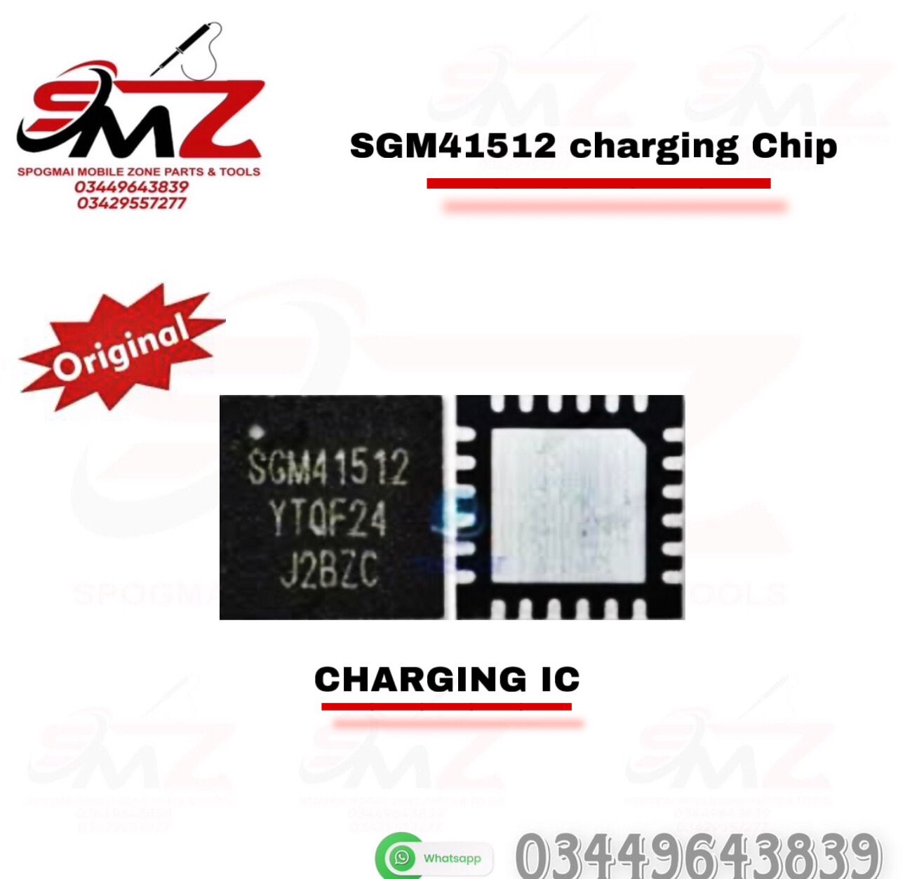
- Package Type: Typically housed in a compact TQFN-24 or BGA package, suitable for high-density space constraints on smartphone motherboards.
🔄 Pin & Functional Compatibility
In mobile repair and circuit design, the SGM41512 is frequently cross-referenced or interchangeable with several other industry-standard power management and charging ICs depending on the specific PCB design layout:
- SGM Variants: Directly related to the SGM41510, SGM41511, SGM41513, and SGM41542 family lines.
- Cross-Brand Alternatives: Frequently shares equivalent footprints or functions with the BQ25601, BQ25601D, BQ21120, and ETA6963 semiconductor chips.




Reviews
There are no reviews yet.